SEM-EDX analysis in Laboratory
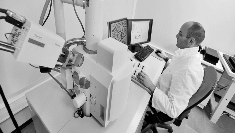
The 6NAPSE Group carries out SEM analysis (Scanning Electron Microscopy). Our laboratory does the observation of all types of materials and calibrated dimensional measurements in order to observe, analyze and assess them.
SEM-EDX analysis
Morphological and elementary characterization of surface and core materials
This equipment makes it possible to quickly provide information on the morphology and the elementary composition of a solid object. Its great ease of use, its flexibility to visualize very variable extension fields on massive samples, the extent of its depth of field make the SEM an indispensable tool in the exploration of the microscopic world.
Our variable pressure means allow the analysis of many materials (plastics, metal, glass, mineral, etc.).
All our SEMs are coupled to an EDX microprobe (X-ray microanalysis) to allow semi-quantitative analyses.
It consists of two coupled devices:
The SEM
Scanning electron microscopy (SEM) is an electron microscopy technique based on the principle of electron-matter interactions, capable of producing high-resolution images of the surface of a sample.
- On the one hand, we have several SEMs with tungsten filament (electron emission by thermoelectric effect) for observation from the macro scale (x5) to the nano scale (x300,000).
- On the other hand, we use Field Emission Gun SEM (FEG-SEM) to achieve a very high spatial resolution of 1nm, ideal for the analysis of nanomaterials. It thus allows the laboratory to extend its field of expertise towards new technologies.
Microanalysis X
The EDX detector receives the photons emitted by the material following the electronic excitation, then sorts them according to their energy. Each energy value being characteristic of an energy level of a chemical element, it is possible to identify the elements contained in matter.
This technique therefore makes it possible to simultaneously obtain morphological (images) and chemical (elementary composition) information from a sample.
Applications
The applications on this means are numerous in view of its capacities. Here is a non-exhaustive list of possibilities:
- Analysis and expertise of polymers
- Glass expertise
- Analysis of an aspect defect
- Fractographic expertise
- Study of corrosion phenomena
- Reliability of mechatronic components
- Layer thickness measurements and elemental analysis of coatings and fillers
- Analysis and identification of foreign bodies (particle, fiber, unknown deposit, filaments, etc.)
- Morphology of metallic, mineral or organic powders
- Characterization of fatigue failure phenomena
- Morphological and elementary characterization of additional fillers of a product (paint for example)
Technical characteristics of our MEB
We are equipped with:
4 tungsten filament SEM (HITACHI S3000N, S3400N, SU3500, JEOL JSM-IT200):
- Magnification up to x 100,000
- Variable pressure -> No metallization on non-conductive samples
- Platine Pelletier: freezing organic samples at -30°C for non-destructive observation
- 2 types of images: topographic contrast (SE mode) and chemical contrast (BSE mode)
1 SEM with field effect gun (FEG-SEM) (JEOL IT700HR/LA)
- Magnification up to x 300,000
- Variable pressure -> No metallization on non-conductive samples
- 2 types of images: topographic contrast (SE mode) and chemical contrast (BSE mode)
EDX UltraDry Detector, Thermo Electron:
- Si crystal, NORVAR window
- Detection from beryllium
- Energy resolution: <132 eV on the K line (Mn)
- Spatial resolution: 1 µm3
For more information, contact our teams!